Concept

The QS series is a QFN style solder-down Computer on Module. It integrates all the core components such as processor, memory and power supply on a small square size of 27mm (QS) or 29mm (QSX) at a maximum overall mounting height below 3mm, soldered onto an application specific carrier board. Its QFN type lead style has a 1mm pitch with 100 (QS) or 108 (QSX) pads. The central ground pad additionally acts as thermal pad.
Feature Overview
Since industrial applications lead to faster, higher integrated and lower power electronic circuits with a smaller formfactor, the PCB layout becomes more and more important. With a good layout many EMI problems can be minimized to meet the required specifications. It’s not only the pinout which should lead to an easy wiring without the need for crossings. It has also to provide a proper solution for the signal path back to the module. If this return path, mostly the ground plane, cannot be connected near the signal pin, the return current has to take another way and this may result in a loop area.
With the special design of KaRo’s QS Series you profit from different advantages.
Large ground pad on the bottom side makes a defined ground plane connection available for all signals.
The pinout leads to an easy wiring without crossings.
Ground will be connected near the signal pin to avoid loop areas.
High speed signals can be routed on the top layer at a defined impedance.
Ground pad holds the component at a defined height during soldering.
EMC Quality by Design

29mm QSX bottom view

27mm QS bottom view
The reason PCB layout becomes more and more important is because of the trend to faster, higher integrated, smaller formfactors, and lower power electronic circuits. The higher the switching frequencies are, the more radiation may occur on a PCB. With good layout, many EMI problems can be minimized to meet the required specifications.
When a module or component is used in a design, the supplier specifies the basis for such a layout. It‘s not only the pinout which should lead to an easy wiring without the need for crossings. He also has to provide a proper solution for the signal path back to the module. If this return path, mostly the ground plane, cannot be connected near the signal pin, the return current has to take another way and this may result in a loop area. The larger the area, the more radiation and EMI problems may occur.
Ka-Ro QS modules uses a large ground pad on the bottom side. With this a defined ground plane connection is available for all signals. In addition to have a good return path for all signals this large ground pad can be used for cooling.
Advanced Soldering
Using a large solder pad underneath the component has not only electrical and thermal advantages. It is also used to hold the component at a defined height during soldering, without the solder being compressed by the weight of the components, which could result in short circuits.
27mm QS - 29mm QSX

QSX is a QS module that has been enlarged by 1mm all around.
The size is hereby increased from 27mm square to 29mm square.
In each corner this gives additional space for a total of 8 further pads which are used for PCIe and USB3.
The inner 27mm x 27mm QS area remains identical providing full compatibility.
Standard Pinout
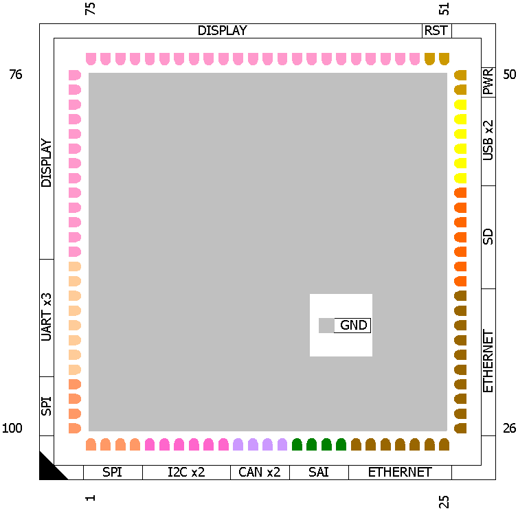
QS Pinout

QSX Pinout
Pins |
Funktion |
QSMP |
QS8M |
QSXM |
QSXP |
|---|---|---|---|---|---|
1-4 |
X |
X |
X |
X |
|
5-10 |
X |
X |
X |
X |
|
11-14 |
X |
X |
|||
19-35 |
X |
X |
X |
X |
|
36-39 |
X |
X |
X |
X |
|
43-48 |
X |
X |
X |
X |
|
49-52 |
X |
X |
X |
X |
|
53-76 |
X |
||||
53-72 |
X |
X |
X |
||
77-78 |
X |
X |
X |
X |
|
79-88 |
X |
X |
X |
X |
|
89-96 |
X |
X |
X |
X |
|
97-100 |
X |
X |
X |
X |
|
1A,75A,76A,100A |
X |
X |
|||
25A,26A,50A,51A |
X |