Optional Debugging Connector
Debug Connector Signal Assignment
Pin |
Signal |
Description |
type |
I/O |
|---|---|---|---|---|
1 |
MFG_NC1 |
Do not connect on the carrier board. These pins are reserved for manufacturing purposes. |
||
3 |
MFG_NC0 |
|||
5 |
BOOT[1] |
Module specific boot mode, refer to the processor datasheet. Boot from flash is selected, if these pins are not connected. (N/A on TX28) |
VDDIO |
I |
7 |
BOOT[0] |
VDDIO |
I |
|
9 |
GND |
|||
11 |
#TRST |
VDDIO |
||
13 |
TMS |
VDDIO |
||
15 |
TDO |
VDDIO |
||
17 |
TDI |
VDDIO |
||
19 |
GND |
|||
21 |
TCK |
VDDIO |
||
23 |
GND |
|||
25, 27, 29 |
NC |
|||
2, 4, 6 … 28, 30 |
GND |
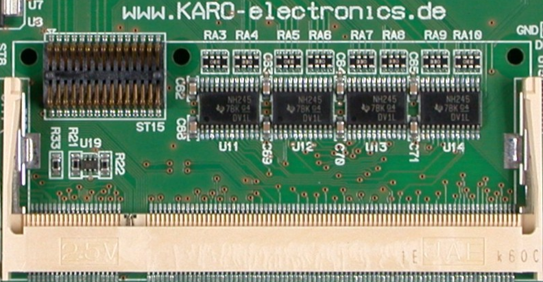
Debug connector location
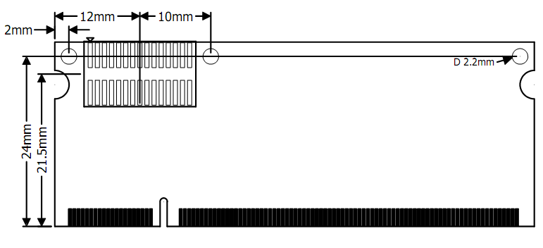
Mates with Samtec FSI - 3mm Height, One Piece Interface, part no. FSI-115-03-G-D-AD
The SO-DIMM connector socket height has to be 5.2mm if the debug connector is used.