Ethernet
Pin |
Signal |
type |
I/O |
Remarks |
19 |
ENET_RST |
3V3 |
OUT |
|
20 |
ENET_CLK125 |
3V3 |
IN |
|
21 |
ENET_INT |
3V3 |
IN |
|
22 |
ENET_MDIO |
3V3 |
I/O |
|
23 |
ENET_MDC |
3V3 |
OUT |
|
24 |
ENET_RXC |
3V3 |
I/O |
|
25 |
ENET_RXCTL |
3V3 |
I/O |
RMII:CRS_DV |
26 |
ENET_RD0 |
3V3 |
I/O |
RMII:RXD0 |
27 |
ENET_RD1 |
3V3 |
I/O |
RMII:RXD1 |
28 |
ENET_RD2 |
3V3 |
IN |
|
29 |
ENET_RD3 |
3V3 |
I/O |
|
30 |
ENET_TXCTL |
3V3 |
I/O |
RMII:TX_EN |
31 |
ENET_TXC |
3V3 |
I/O |
|
32 |
ENET_TD3 |
3V3 |
IN |
|
33 |
ENET_TD2 |
3V3 |
I/O |
|
34 |
ENET_TD1 |
3V3 |
I/O |
RMII:TXD1 |
35 |
ENET_TD0 |
3V3 |
I/O |
RMII:TXD0 |
Wiring example
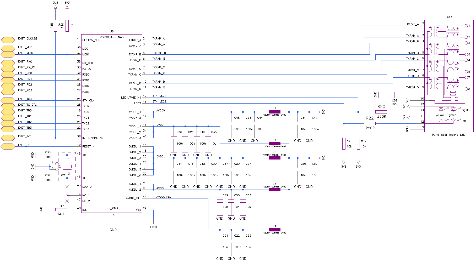
RGMII Timing (KSZ9031RNX Gigabit Ethernet PHY)
As the default, after power-up or reset, the KSZ9031RNX RGMII timing conforms to the timing requirements in the RGMII Version 2.0 Specification for internal PHY chip delay.
For the transmit path (MAC to KSZ9031RNX), the KSZ9031RNX does not add any delay locally at its GTX_CLK, TX_EN and TXD[3:0] input pins, and expects the GTX_CLK delay to be provided on-chip by the MAC. If MAC does not provide any delay or insufficient delay for the GTX_CLK, the KSZ9031RNX has pad skew registers that can provide up to 1.38ns on-chip delay.
For the receive path (KSZ9031RNX to MAC), the KSZ9031RNX adds 1.2ns typical delay to the RX_CLK output pin with respect to RX_DV and RXD[3:0] output pins. If necessary, the KSZ9031RNX has pad skew registers that can adjust the RX_CLK on-chip delay up to 2.58ns from the 1.2ns default delay.
It is common to implement RGMII PHY-to-MAC designs that either PHY, MAC, or both PHY and MAC are not fully RGMII v2.0 compliant with on-chip clock delay. These combinations of mixed RGMII v1.3/v2.0 designs and plus sometimes non-matching RGMII PCB trace routings require a review of the entire RGMII system timings (PHY on-chip, PCB trace delay, MAC on-chip) to compute the aggregate clock delay and determine if the clock delay timing is met. If timing adjustment is needed, pad skew registers are provided by the KSZ9031RNX. Refer to RGMII Pad Skew Registers section.
RGMII v2.0 Specification
Parameter |
MIN |
TYP |
MAX |
Data to clock output skew (at transmitter) per RGMII v1.3 (external delay) |
-500ps |
500 ps |
|
Data to clock input skew (at receiver) per RGMII v1.3 (external delay) |
1 ns |
2.6 ns |
|
Data to clock output setup (at transmitter – integrated delay) |
1.2 ns |
2ns |
|
Data to clock output setup (at transmitter – integrated delay) |
1.2 ns |
2ns |
The RGMII Version 2.0 Specification defines the RGMII data-to-clock skews only for 1000Mbps operation, which usesboth clock edges for sampling the data and control signals at the 125MHz clock frequency (8ns period). For 10/100Mbps operations, the data signals are sampled on the rising clock edge and the control signals are sampled on both clock edges. With slower clock frequencies, 2.5MHz (400ns period) for 10Mbps and 25MHz (40ns period) for 100Mbps, the RGMII data-to-clock skews for 10/100Mbps operations will have greater timing margins than for 1000Mbps operation, and therefore can be relaxed from 2.6ns (maximum) for 1000Mbps to 160ns (maximum) for 10Mbps and 16ns (maximum) for 100Mbps
See also
Microchip KSZ9031RNX datasheet
Microchip AN-111 General PCB Design and Layout Guidelines
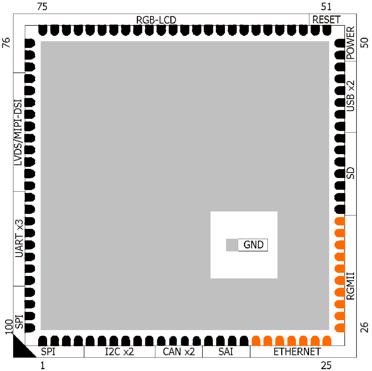
QS Standard Contact Group Index
Pins |
Function |
Pins |
Function |
Pins |
Function |
Pins |
Function |
|---|---|---|---|---|---|---|---|
1-4 |
5-10 |
11-14 |
15-18 |
||||
19-35 |
36-42 |
43-48 |
49-52 |
||||
53-76 |
77-78 |
53-72 |
79-88 |
||||
89-96 |
97-100 |
1A,75A,76A,100A |
25A,26A,50A,51A |