USB
Pin |
Signal |
Description |
type |
I/O |
|||
|---|---|---|---|---|---|---|---|
27 34 |
USBH_VBUSEN USBOTG_VBUSEN |
This pin is used to enable the external VBUS power supply. |
3V3 |
O |
|||
28 36 |
#USBH_OC #USBOTG_OC |
Active low over-current indicator input connected to a GPIO. This signal can be used as an input only. |
3V3 |
I |
|||
30 38 |
USBH_VBUS USBOTG_VBUS |
VBUS pin of the USB cable. This pin is used for the VBUS comparator inputs. |
5V |
I |
|||
Module |
Remark |
||||||
TX25 |
USBH_VBUS / USBOTG_VBUS unused / Not connected |
||||||
TX28 |
USBH_VBUS unused / Not connected |
||||||
31 29 |
USBH_DP USBH_DM |
USB Host port differential data signal |
USB |
I/O |
|||
37 35 |
USBOTG_DP USBOTG_DM |
USB OTG port differential data signal |
USB |
I/O |
|||
33 |
USBOTG_ID |
ID pin of the USB cable. For an A-Device ID is grounded. For a B-Device ID is floated. |
5V |
I |
|||
Module |
Remark |
||||||
TX25/TX28/TX48/TX53/TX6 |
USBOTG_VBUSEN, USBOTG_OC are also used for the 2nd CAN interface. In that case the VBUSEN/OC functionality may be omitted or other GPIO’s may be used instead. |
||||||
USB Physical Layer Layout Guidelines
The TX modules includes the physical layer interface (PHY) for systems using Hi-Speed USB. Proper design techniques must be used in printed circuit board (PCB) layout to maintain the signal integrity required for 480 Mbps operation.
Controlled Impedance for USB Traces
The USB 2.0 specification requires that the USB DP/DM traces maintain a nominal 90 Ohms +/- 15% differential impedance (see USB specification Rev. 2.0, paragraph 7.1.1.3 for more details). In the example design the traces are 7 mil (175um) wide with line spacing of 7 mils. These numbers are derived for 5 mil (125um) distance from ground reference plane. A continuous ground plane is required directly beneath the DP/DM traces and extending at least 5 times the spacing width to either side of DP/DM lines. Maintain symmetry between DP/DM lines in regards to shape and length. Single sided impedance is not as critical as differential impedance. A range of 42 to 78 Ohms is acceptable (equivalently, common mode impedance must be between 21 Ohms and 39 Ohms).
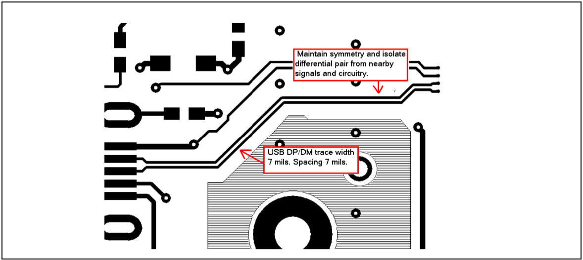
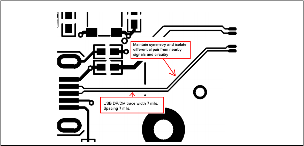
The figures show DP/DM traces with approximately equal trace length and symmetry. It is important to maintain a conductor width and spacing that provides differential and common mode impedance compliant with the USB specification. Use 45 degree turns to minimize impedance discontinuities.
Isolation of DP/DM Traces
The DP/DM lines must be isolated from nearby circuits and signals. Maintain a distance of components to lines that is greater or equal to 5 times the distance of the spacing between the traces. Do not route differential pairs under components. Do not cross DP/DM lines with other PCB traces unless the traces are on the opposite side of the ground plane from DP/DM. Route DP/DM over solid ground plane with no ground plane splits under the traces.
Isolated shielding on the USB connector
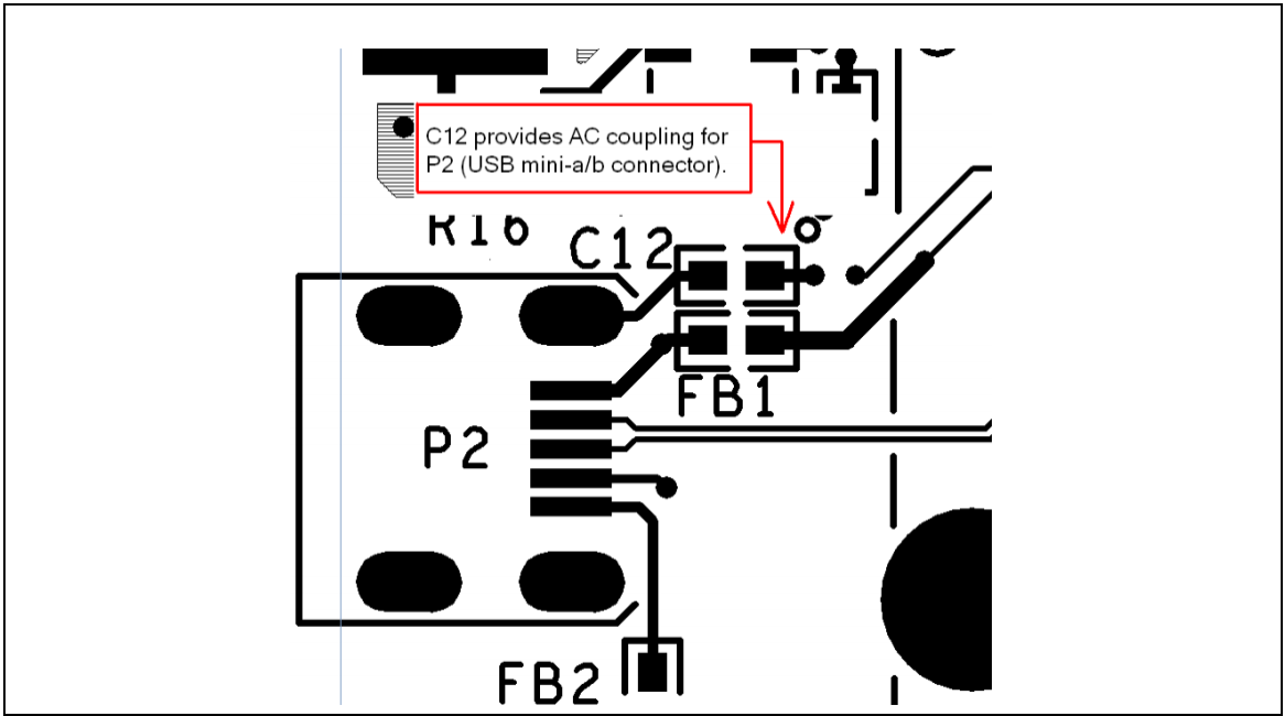
The figure shows the Mini-AB connector housing is isolated but AC coupled to the device ground. Industry convention is to ground only the host side of the cable shield. This is done to provide cable shielding while preventing possible ground currents from flowing in the USB cable if there happens to be a potential difference between the host and device grounds. If DC grounding is required replace C12 with a zero Ohms resistor. In OTG applications the shield may be DC grounded at both ends of the cable.
USB recommendations [1]
- In summary use the following recommendations for the USB.
Route DP and DM signals on the top or bottom layer of the board
The trace width and spacing of the DP and DM signals should be such that the differential impedance is 90 Ω.
Route traces over continuous planes (power and ground).
They should not pass over any power/GND plane slots or anti-etch.
When placing connectors, make sure the ground plane clearouts around each pin have ground continuity between all pins.
Maintain the parallelism (skew matched) between DP and DM; these traces should be the same overall length.
Do not route DP and DM traces under oscillators or parallel to clock traces and/or data buses.
Minimize the lengths of high speed signals that run parallel to the DP and DM pair.
Keep DP and DM traces as short as possible.
Route DP and DM signals with a minimum amount of corners. Use 45-degree turns instead of 90-degree turns.
Avoid layer changes (vias) on Dm and Dp signals. Do not create stubs or branches.