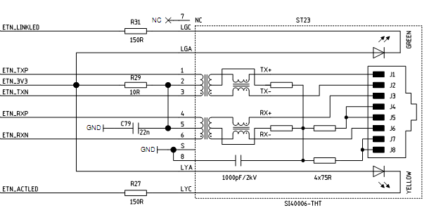
Ethernet Signals
Pin |
Signal |
Description |
type |
I/O |
||||
|---|---|---|---|---|---|---|---|---|
19 21 |
ETN_TXN ETN_TXP |
100Base-TX or 10Base-T differential transmit output to magnetics. |
ETN |
O |
||||
20 |
#ETN_LINKLED |
Active low LINK ON indication: Active indicates that the link is on. |
3V3 |
O |
||||
Module |
Remark |
|||||||
TX28, TX48, TX53, TX6 |
Output is driven active when the operating speed is 100Mbps. This LED will go inactive when the operating speed is 10Mbps or during line isolation. |
|||||||
22 |
ETN_3V3 |
+3.3V analogue power supply output to magnetics. This power supply can be turned off on the module to reduce the power consumption in the case Ethernet is not needed. |
power |
O |
||||
23 25 |
ETN_RXN ETN_RXP |
100Base-TX or 10Base-T differential receive input from magnetics. |
ETN |
I |
||||
24 |
#ETN_ACTLED |
Active low ACTIVITY indication: Active indicates that there is Carrier sense (CRS) from the active PMD. |
3V3 |
O |
||||
Module |
Remark |
|||||||
TX28, TX48, TX53, TX6 |
Output is driven active whenever the device detects a valid link, and blinks indicating activity. |
|||||||
Ethernet Physical Layer Layout Guidelines
TX modules are designed for 10 or 100 Mbps Ethernet systems. They are based on IEEE 10BASE-T and 100BASE-TX standards. The IEEE 802.3-2005 standard for 100BASE-TX defines networking over two pairs of Category 5 unshielded twisted pair cable or Type 1 shielded twisted pair cable. The following recommendations for the printed circuit board layout are not the only way to layout TX modules. Every board designer will have a preference. Complexity, board space, number and types of devices will dictate routing and placement strategies.
Power and Ground Planes
The sections below describe typical 2 and 4 layer board stackups. The goal of the 4 layer designs is to keep the signal routing on outer layers, isolated by the power and ground planes. These power and ground planes also serve the purpose of reference planes for the signal traces. The signal traces should run over continuous reference planes when possible. When 2 layer board designs are required, it remains necessary that the signal traces run over continuous reference planes when possible.
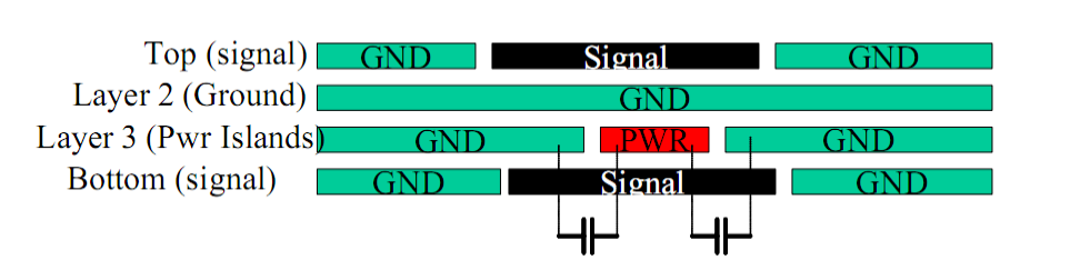
4 Layer Stackup
TOP (Layer 1) – Signal with ground plane except where noted.
Layer 2 – Continuous ground plane. No signals should be routed on this layer.
Layer 3 – Power planes with ground planes except where noted. Signals may be routed on this layer if needed.
Bottom (Layer 4) – Signal with ground plane except where noted.
Decouple ground floods and ground layer as practical. When signal traces are re-referenced to power island planes, decoupling capacitors (10nF ceramic) are required between the ground plane and power plane.
Signal traces routed on bottom layer over power islands that are on Layer 3 layer should have decoupling capacitors (10nF ceramic) near the trace to enable short (direct) return current paths.
When signal traces are re-referenced to power island planes, decoupling capacitors (10nF ceramic) are required between the ground plane and power plane as shown below.
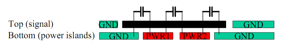
2 Layer Stackup
TOP (Layer 1) – Signal with ground plane except where noted.
Bottom (Layer 1) – Ground plane and power islands. A limited number of slow speed signals may be routed on the bottom layer.
Signal traces should be surrounded by ground or ground trace along at least one edge. If ground trace is used, it should be connected to ground plane on this layer and decoupled to ground plane on top layer. Decouple ground planes as practical , as shown below. This will allow short (direct) return current paths when signal traces are re-referenced to different power island planes.
Component Placement
Component placement can affect signal quality, emissions, and component operating temperature. Careful component placement can decrease potential EMI problems and simplify the task of routing traces.
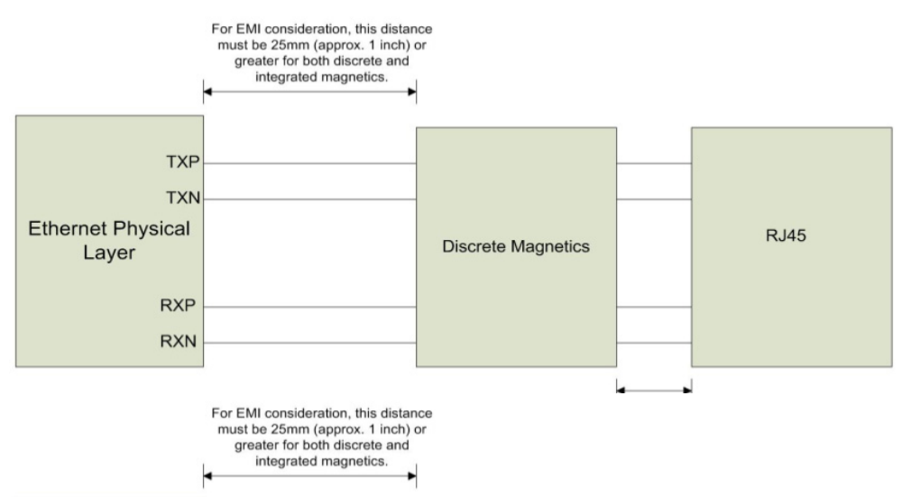
If the magnetic is a discrete component, then the distance between the magnetic and the RJ-45 needs to have the highest consideration and be kept to under 25mm (approx. 1 inch) of separation.
The distance between the SO-DIMM socket and the magnetics needs to be 20mm or greater. Among PHY vendors, the 25mm (approx. 1 inch) rule is considered good design practice for EMI considerations. The intention is to isolate the PHY from the magnetics.
Design Techniques for EMI Suppression
The following techniques may improve EMI margin.
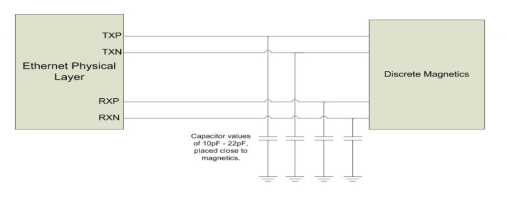
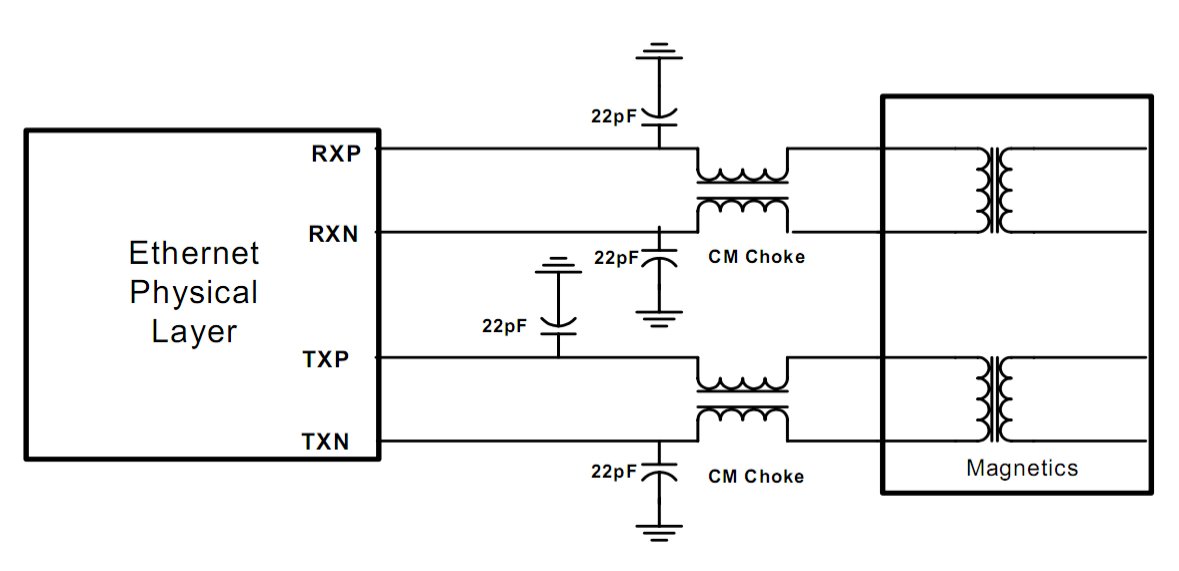
Common mode capacitors may be added to the TX+/- and RX+/- signals for high frequency attenuation , as shown below. One end of each capacitor should be connected to the system ground plane, and placed within 10mm (approx. 400mils) of the magnetics. Typical capacitance values should be between 10pF and 22pF. Values higher than 22pF may negatively impact the TX and RX signalling.
Common mode chokes may be added to the TX and RX differential pairs as shown below. The common mode chokes should be placed within 10mm (approx. 400mils) of the integrated RJ45 module, and on the magnetics side of the common mode EMI suppression capacitors. Typical common mode impedance of the common mode choke selected should be 2kΩ@100MHz or higher.
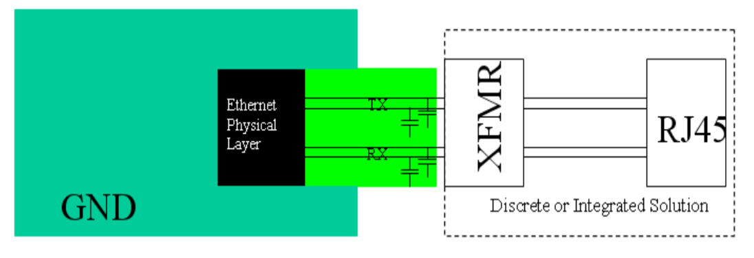
In general, no ground plane should extend under the TX and RX differential pairs, under the magnetics, or under the RJ45 jack. In the case where common mode capacitors used for EMI suppression, a ground plane may be located under the TX and RX signals, however the plane must not exceed beyond the capacitors. When designing 4 layer boards, the ground plane should exist on layer 4, assuming the differential pair is routed on layer 1. On 2 layer boards, the ground plane can be located on layer 2, the adjacent layer to the TX and RX signal pairs. Under no circumstances should a ground plane exist under the magnetics, the RJ45 connector or in between the magnetics and RJ45 connector.
Controlled Impedance for Differential Signals
The 802.3-2005 specifications requires the TX and RX lines to run in differential mode. The TXP and TXN are a differential pair and need to be designed to a 100 ohm differential impedance. The RXP and RXN traces are also a differential pars and need to be designed to a 100 ohm differential impedance target.
The board designer must maintain 100 ohm differential impedance in the layout for all differential pairs. For differential dielectric thickness, copper weight or board stack-up, trace width and spacings will need to be calculated.
Differential pair nets must maintain symmetry. TXP and TXN must be equal length and symmetric with regards of shape, length, and via count. RXP and RXN must also be equal length and symmetric.
Isolation of TX/RX traces. The TX/RX traces must be isolated from nearby circuitry and signals. Maintain a distance of parts to lines that are greater than or equal to 5 times the distance of the spacing between the traces. Do not route differential pairs under parts. Do not cross TX/RX lines with other PCB traces unless the traces are on the opposite side of the ground plane from TX/RX.
Magnetics Module
The magnetics module has a critical effect on overall IEEE and emissions conformance. The device should meet the performance required for a design with reasonable margin to allow manufacturing variation. Occasionally, components that meet basic specifications may cause the system to fail IEEE testing, because of interactions with other components or the Printed Circuit Board itself. Carefully qualifying new magnetics modules can go a long way toward preventing this type of problem.
Suggested magnetics have not been tested in order to verify proper operation. This category of magnetic has been evaluated by the contents of the vendor supplied data sheet and legacy performance only. However, the designer can assume with some degree of confidence, that with proper PCB design techniques, the magnetics presented as suggested magnetics will perform to high standards.
Qualified magnetics have been tested by the PHY vendor in order to verify proper operation. The designer can assume with a high degree of confidence, that with proper PCB design techniques, the qualified magnetics perform to the highest standards.
Vendor |
Part number |
Package |
Temp |
Status |
|---|---|---|---|---|
Pulse |
H1102 |
16-pin SOIC |
0°..+70°C |
Qualified |
Halo |
TG110-RP55N5 |
16-pin SOIC |
0°..+70°C |
Qualified |
Halo |
HFJ11-RP26E-L12RL |
Integrated RJ45 |
0°..+70°C |
Qualified |
Delta |
RJSE1R5310A |
Integrated RJ45 |
0°..+70°C |
Qualified |
Pulse |
J0011D01B |
Integrated RJ45 |
0°..+70°C |
Suggested |
Bothhand |
TS6121C |
16-pin SOIC |
0°..+70°C |
Suggested |
Bothhand |
LU1S041X-43 |
Integrated RJ45 |
0°..+70°C |
Suggested |
Pulse |
HX1102 |
16-pin SOIC |
-40°..+85°C |
Qualified |
Halo |
TG110-RPE5N5 |
16-pin SOIC |
-40°..+85°C |
Qualified |
Halo |
HFJ11-RPE26E-L12RL |
Integrated RJ45 |
-40°..+85°C |
Qualified |
TDK |
TLA-6T717W |
Integrated RJ45 |
-40°..+85°C |
Qualified |
Delta |
LFE8505T |
16-pin SOIC |
-40°..+85°C |
Qualified |
Midcom |
000-7090-37R |
16-pin SOIC |
-40°..+85°C |
Suggested |
Midcom |
MIC66211-5171T-LF3 |
Integrated RJ45 |
-40°..+85°C |
Suggested |
Elec & Eltek |
820-M0323R |
16-pin SOIC |
-40°..+85°C |
Suggested |
Midcom / Würth-Elektronik |
MIC24013-5101T-LF3 /749 901 121 11 |
Integrated RJ45 |
0°..+70°C |
Used on Starterkit 5 |
Bel Stewart |
SI-60005-F |
Integrated RJ45 |
N/A |
Used on Starterkit 5 |